HOME Business Description Corporate Philosophy Products Contact us News

Products


TopProducts(Semiconductor)
@@Solar cell Semiconductor
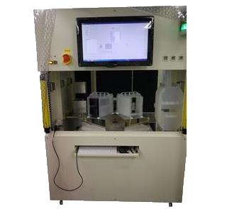
Wafer Suface Automatic Inspection System

This inspection system automatically detects defects on the wafer surface. From visual inspection by the operator corresponds to automation of inspection system. We can suggest the optimum system by actually imaging and inspecting the detection target.

specification

Wafer size 200mm@OF, V Notch
Wafer transportation method

Back side adsorption method

System configuration ETransportation unit
ELoader / unloader unit
EAlignment unit
ESurface inspection unit
EUpward communication function (option)
Dimension

1250(W)~1700(D)~1800(H) mm

* This dimension doesn't contain the height of the protrusion.

* This is an example of the product specification. We supports customized specifications.